Trace PIB Sink
Trace data may be sent to chip pins through an interface called the Pin Interface Block (PIB). This interface typically operates at a few hundred MHz and can sometimes be higher with careful constraints and board layout or by using LVDS or other high-speed signal protocol. PIB may consist of just one signal and in this configuration may be called SWT (Serial-Wire Trace). Alternative configurations include a trace clock (TRC_CLK) and 1/2/4/8/16 parallel trace data signals (TRC_DATA) timed to that trace clock. WARL register fields are used to determine specific PIB capabilities.
The modes and behavior described here are intended to be compatible with trace probes available in the market.
PIB Register Interface
| Bit | Field | Description | RW | Reset |
|---|---|---|---|---|
0 |
trPibActive |
Primary activate/reset bit for PIB Sink component. When 0, the PIB Sink may have clocks gated off or be powered down, and other register locations may be inaccessible. Hardware may take an arbitrarily long time to process power-up and power-down and will indicate completion when the read value of this bit matches what was written. See Reset and Discovery chapter for more details. |
RW |
0 |
1 |
trPibEnable |
0: PIB does not accept input but holds output(s) at idle state defined by pibMode. |
RW |
0 |
2 |
— |
Reserved |
— |
0 |
3 |
trPibEmpty |
Reads 1 when PIB internal buffers are empty. |
RO |
1 |
7:4 |
trPibMode |
Select mode for output pins. Allowed values are described in the |
WARL |
|
8 |
trPibClkCenter |
In parallel modes, adjust TRC_CLK timing to the center of the bit period. This can be set only if |
WARL |
|
9 |
trPibCalibrate |
Set this to 1 to generate a repeating calibration pattern to help tune a probe’s signal delays, bit rate, etc. In this mode input to the sink is not consumed. The calibration pattern is described below. |
WARL |
|
11:10 |
— |
Reserved |
— |
0 |
14:12 |
trPibAsyncFreq |
0: Alignment synchronization (Async) packets disabled (may be the only choice for some protocols) |
WARL |
|
15 |
— |
Reserved |
— |
0 |
31:16 |
trPibDivider |
Timebase selection for the PIB module. The input clock is divided by |
WARL |
| Bit | Field | Description | RW | Reset |
|---|---|---|---|---|
3:0 |
trPibVerMajor |
Trace PIB Sink Component Major Version. Value 1 means the component is compliant with this document. |
RO |
1 |
7:4 |
trPibVerMinor |
Trace PIB Sink Component Minor Version. Value 0 means the component is compliant with this document. |
RO |
0 |
11:8 |
trPibCompType |
Trace PIB Sink Component Type (PIB Sink) |
RO |
0xA |
23:12 |
— |
Reserved for future versions of this standard |
— |
0 |
31:24 |
— |
Reserved for vendor specific implementation details |
— |
Software can determine what modes are available by attempting to write each mode setting to the WARL field trPibMode and reading back to see if the value was accepted.
| Mode | trPibMode | trPibClkCenter | Bit rate |
|---|---|---|---|
Off |
0 |
X |
— |
SWT Manchester |
4 |
X |
1/2 |
SWT UART |
5 |
X |
1 |
TRC_CLK + 1 TRC_DATA |
8 |
0 |
1 |
TRC_CLK + 2 TRC_DATA |
9 |
0 |
1 |
TRC_CLK + 4 TRC_DATA |
10 |
0 |
1 |
TRC_CLK + 8 TRC_DATA |
11 |
0 |
1 |
TRC_CLK + 16 TRC_DATA |
12 |
0 |
1 |
TRC_CLK + 1 TRC_DATA |
8 |
1 |
1/2 |
TRC_CLK + 2 TRC_DATA |
9 |
1 |
1/2 |
TRC_CLK + 4 TRC_DATA |
10 |
1 |
1/2 |
TRC_CLK + 8 TRC_DATA |
11 |
1 |
1/2 |
TRC_CLK + 16 TRC_DATA |
12 |
1 |
1/2 |
Since the PIB supports many different modes, it is necessary to follow a particular programming sequence:
-
Activate the PIB by setting
trPibActive. -
Set the
trPibMode,trPibDivider,trPibClkCenter, andtrPibCalibratefields. This will set the TRC_DATA outputs to the quiescent state (whether that is high or low depends ontrPibMode) and start TRC_CLK running. -
Activate the receiving device, such as a trace probe. Allow time for PLL to sync up, if using a PLL with a parallel PIB mode.
-
Set
trPibEnable. This enables the PIB to generate output either immediately (calibration mode) or when the Trace Encoder or Trace Funnel begins sending trace messages/packets.
Order of bits and bytes
-
Trace messages/packets are considered as sequences of bytes and are always transmitted with least significant bits/bytes first.
-
In 16-bit mode (
trPibMode== 12) the byte transmitted on bits #0-#7 is considered first and most significant bits#8-#15 are transmitting second byte. -
Idle sequences (no message/packet to be sent) are transmitted between messages.
-
Idle sequence depends on trace protocol and must allow detection of the start of first byte of message/packet following the idle sequence.
-
Idle sequences may be different and should be defined by trace protocols.
-
PIB Parallel Protocol
Traditionally, off-chip trace has used this protocol. There are several parallel data signals (TRC_DATA0..15) and one continuously-running trace clock (TRC_CLK). The data rate of parallel signals can be much higher than either of the serial-wire protocols.
This protocol is oriented to send full, variable length trace messages/packets rather than fixed-width trace words.
When a message start is detected, this sample and possibly the next few (depending on the width of TRC_DATA) are collected until a complete byte has been received. Bytes are transmitted least significant bit first, with TRC_DATA[0] representing the least significant bit in each beat of data. The receiver continues collecting bytes until a complete message has been received. The criteria for this depends on the trace format. After the last byte of a message, the data signals may then go to their idle state or a new message may begin in the next trace clock edge.
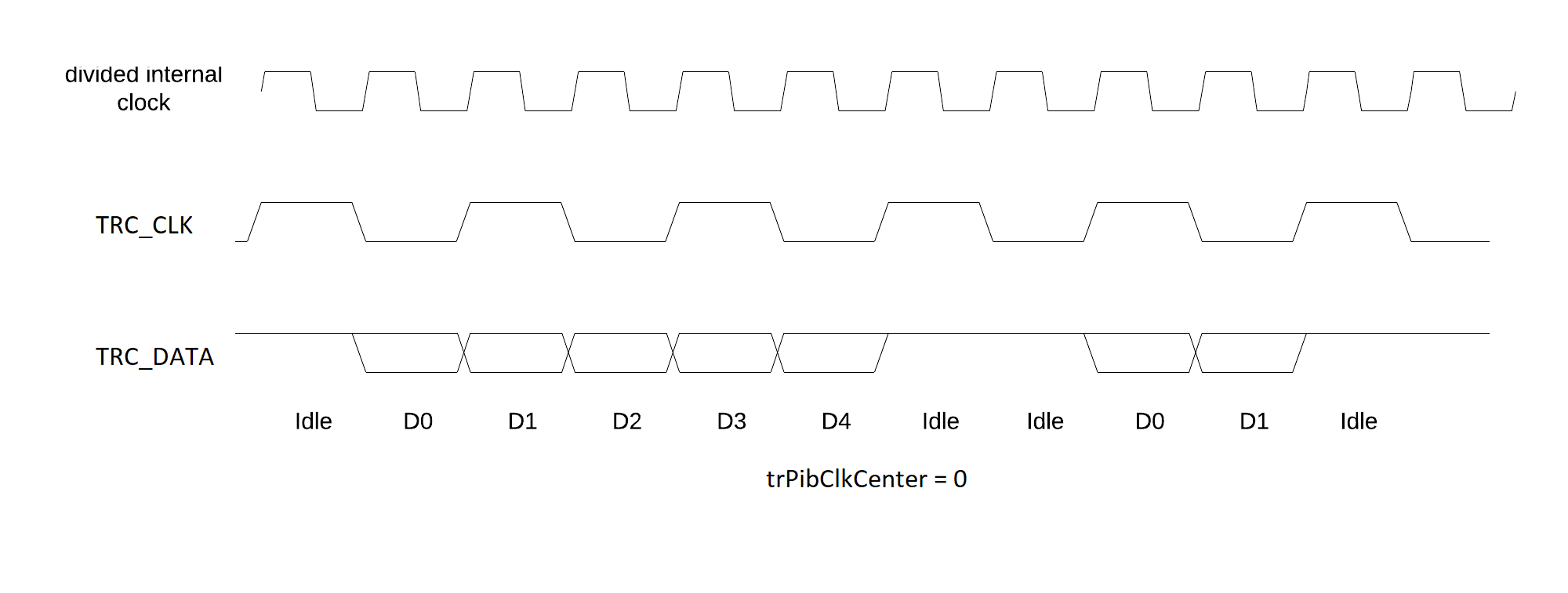
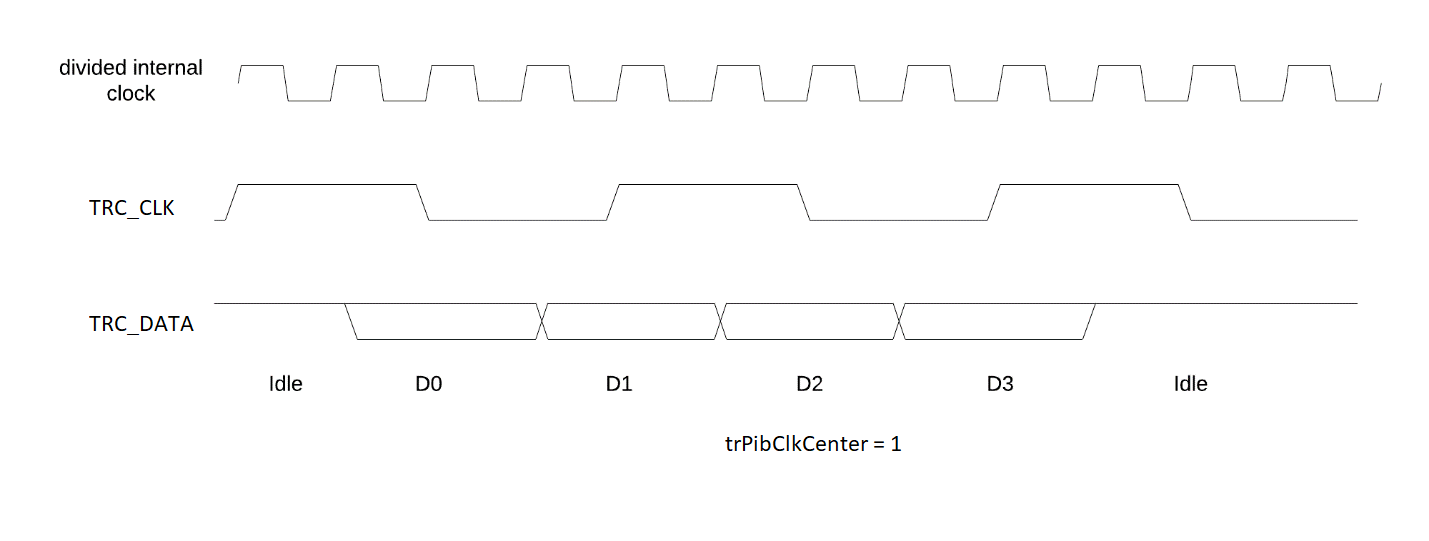
PIB Clock Center
The trace clock, TRC_CLK, normally has edges coincident with the TRC_DATA edges. Typically, a trace probe will delay trace data or use a PLL to recover a sampling clock that is twice the frequency of TRC_CLK and shifted 90 degrees so that its rising edges occur near the center of each bit period. If the PIB implementation supports it, the debugger can set trPibClkCenter to change the timing of TRC_CLK so that there is a TRC_CLK edge at the center of each bit period on TRC_DATA. Note that this option cuts the data rate in half relative to normal parallel mode and still requires the probe to sample TRC_DATA on both edges of TRC_CLK.
This example shows 8-bit parallel mode with trPibClkCenter = 0 transmitting a 5-byte message/packet followed by a 2-byte message/packet.
And an example showing 8-bit parallel mode transmitting a 4-byte packet with trPibClkCenter = 1
SWT Manchester Protocol
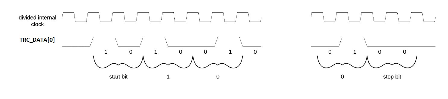
In this mode, the PIB outputs complete trace messages encapsulated between a start bit and a stop bit. Each bit period is divided into 2 phases and the sequential values of the TRC_DATA[0] pin during those 2 phases denote the bit value. Bits of the message are transmitted LSB first. The idle state of TRC_DATA[0] is low in this mode.
| Bit | Phase 1 | Phase 2 |
|---|---|---|
start |
1 |
0 |
logic 0 |
0 |
1 |
logic 1 |
1 |
0 |
stop/idle |
0 |
0 |
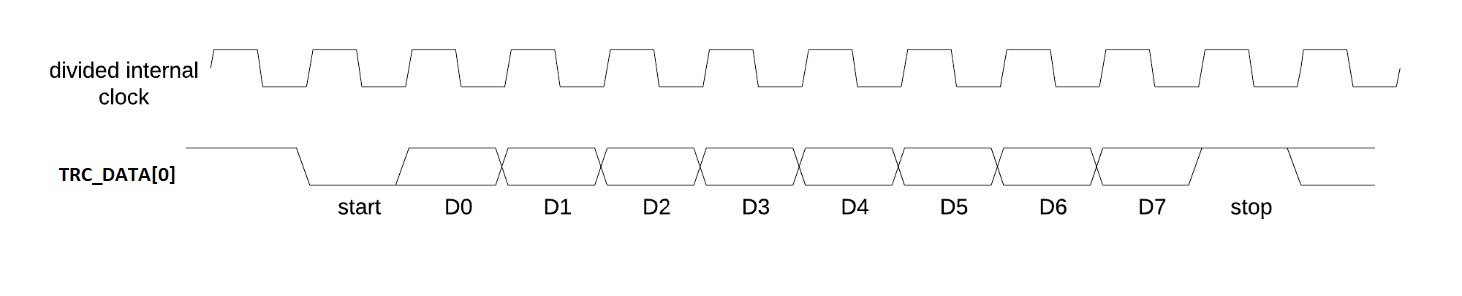
SWT UART Protocol
In UART protocol, the PIB outputs bytes of a trace message encapsulated in a 10-bit packet consisting of a low start bit, 8 data bits, LSB first, and a high stop bit. Another packet may begin immediately following the stop bit or there may be an idle period between packets. When no data is being sent, TRC_DATA[0] is high in this mode.
Calibration Mode
In optional calibration mode, the PIB transmits a repeating pattern. Probes can use this to automatically tune input delays due to skew on different PIB signal lines and to adjust to the transmitter’s data rate (trPibDivider and trPibClkCenter). Calibration patterns for each mode are listed below.
| Mode | Calibration Bytes | Wire Sequence |
|---|---|---|
UART, Manchester |
AA 55 00 FF |
alternating 1/0, then all 0, then all 1 |
1-bit parallel |
AA 55 00 FF |
alternating 1/0, then all 0, then all 1 |
2-bit parallel |
66 66 CC 33 |
2, 1, 2, 1, 2, 1, 2, 1, 0, 3, 0, 3, 3, 0, 3, 0 |
4-bit parallel |
5A 5A F0 0F |
A, 5, A, 5, 0, F, F, 0 |
8-bit parallel |
AA 55 00 FF |
AA, 55, 00, FF |
16-bit parallel |
AA AA 55 55 00 00 FF FF |
AAAA, 5555, 0000, FFFF |
| Calibration mode may be used even by probes which do not support calibration of trace just to assure trace routing on PCB is correct and PIB is correctly enabled. It may be also possible to use calibration mode to check trace signal routing from SoC using scope or logic analyzer. |